

Grain Boundary Effects on the Mobility of Chemical Vapor Deposition Synthesized Monolayer MoS2-FETs
JU Qian-Kun, HONG Wen-Ting and LIU Wei*
Chin. J. Struct. Chem. 2021, 40, 512-518 DOI: 10.14102/j.cnki.0254-5861.2011-2934
April 15, 2021
grain boundary, golybdenum disulfide, ghemical vapor deposition, field-effect transistor
ABSTRACT
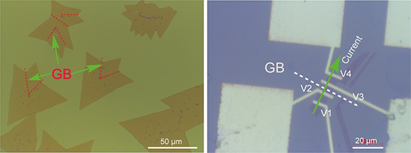
Molybdenum disulphide (MoS2)
has emerged as a promising candidate for low-power digital applications.
However, grain boundaries play a decisive role in determining the carrier
mobility and performance of MoS2-FETs. In this work, we report a
systematic study on the grain boundary of chemical vapor deposition (CVD) MoS2. We found that in the
ON-state, if current flows across a grain boundary that is aligned
perpendicular to the channel length, the current of CVD MoS2-FETs
can be significantly reduced, while in the OFF-state, the effect is negligible.
Metal-insulator-transition is clearly observed, indicating the high quality of our CVD samples, and
it is also shown that grain boundaries increase the metal-insulator-transition
crossover-voltage in MoS2-FETs. Thereby, this work provides useful
information and guidance in understanding the nature of carrier transport in
synthesized MoS2 devices, and the developed framework can be applied
to other 2D semiconductors in general, as well as in optimizing the CVD
process and device design with 2D materials.


- Address: Fuzhou High & New Technology Industrial Zone, Shangjie, Minhou, Fuzhou, Fujian 350108, China
- Tel: (86)-591-63173769, 63173770
- E-mail: cjsc@fjirsm.ac.cn
CN 35–1112/TQ, ISSN 0254–5861, Online ISSN: 2949-768X Copyright @ 2022 Chinese Journal of Structural Chemistry-www.Chinese Journal of Structural Chemistry.net. All Rights Reserved 闽ICP备2022002645号-1